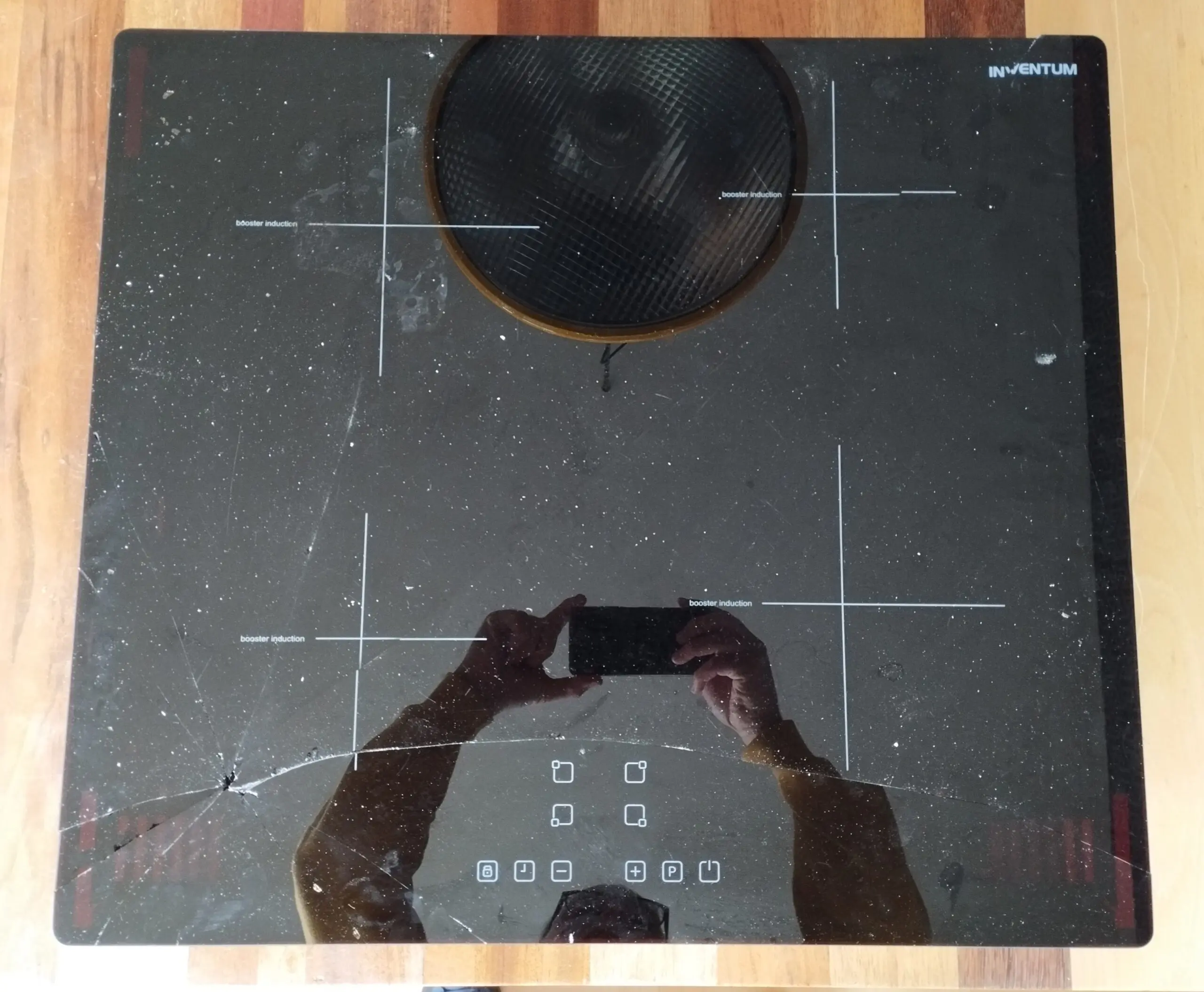
I received a broken Inventum IKI6010 induction stove, a bottle of olive oil was dropped on the glass-ceramic surface which as a result got broken. I have the same make and model installed in my kitchen and am wondering, can I fix it (that should be easy), what’s inside and can it be made smart? Let’s investigate!
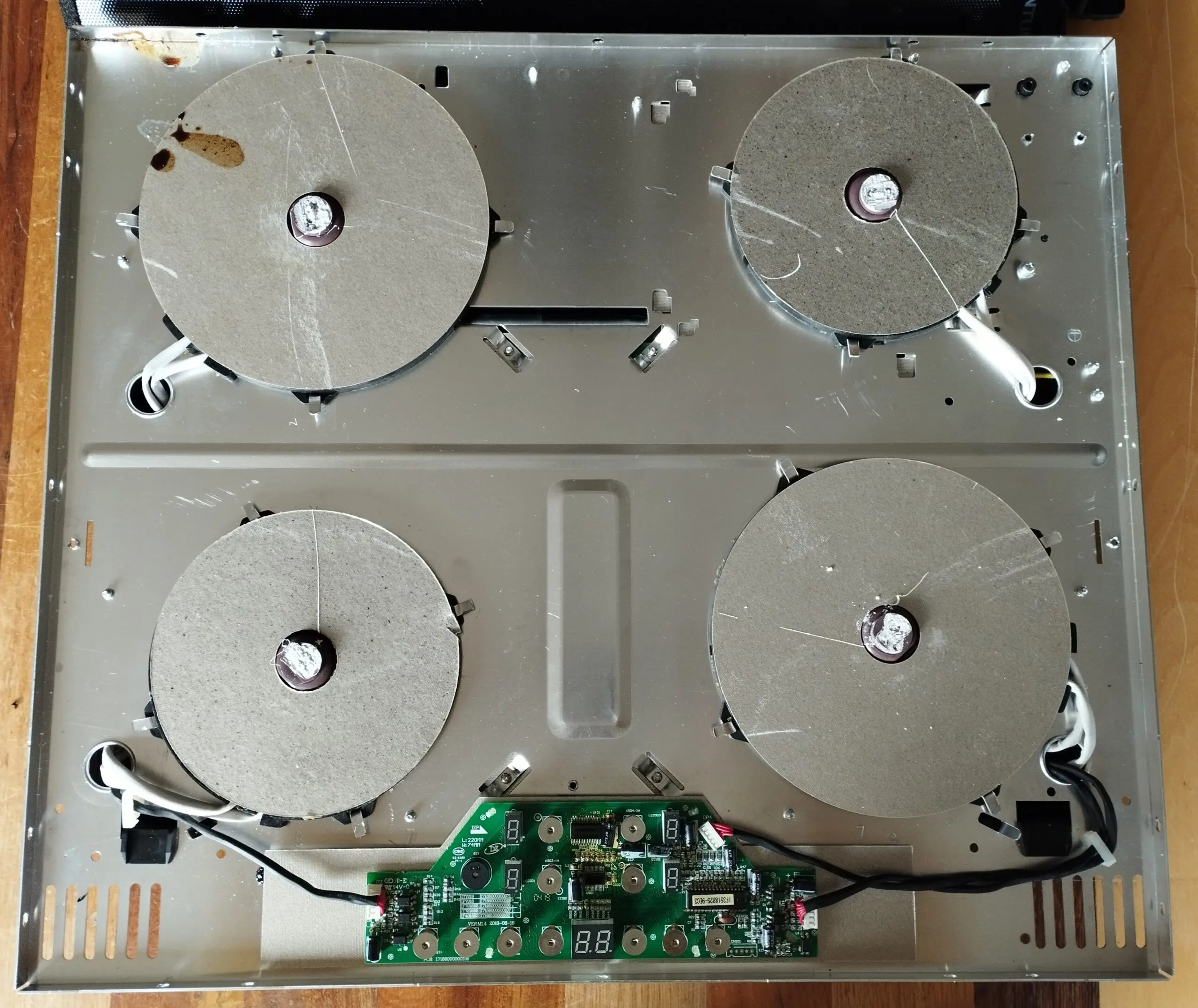
Removing the glass top reveals the 4 induction coils and the control PCB.
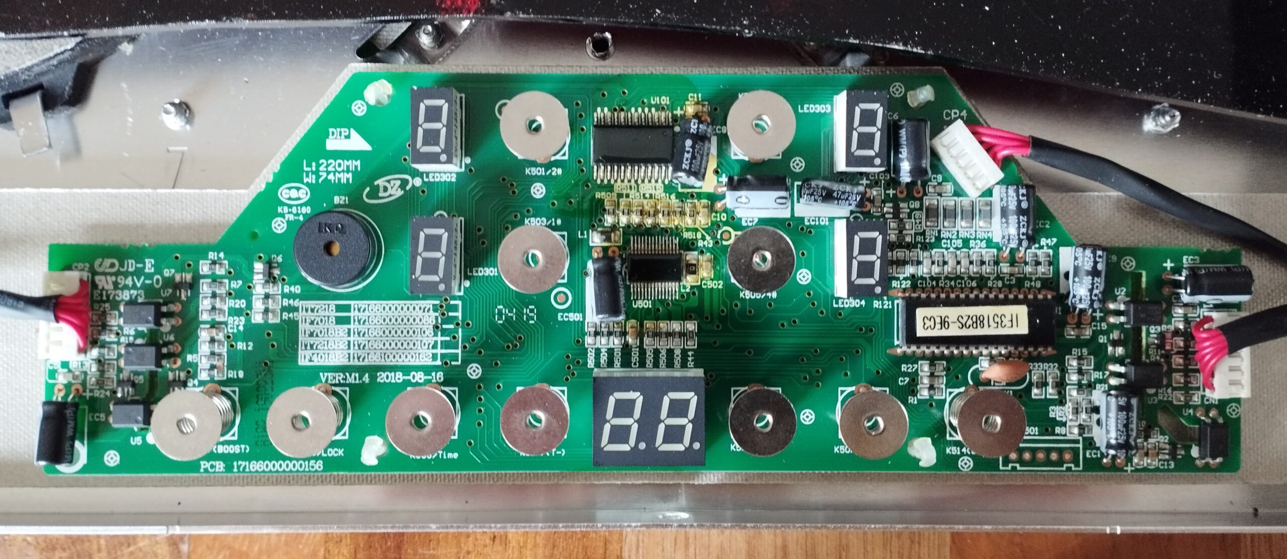
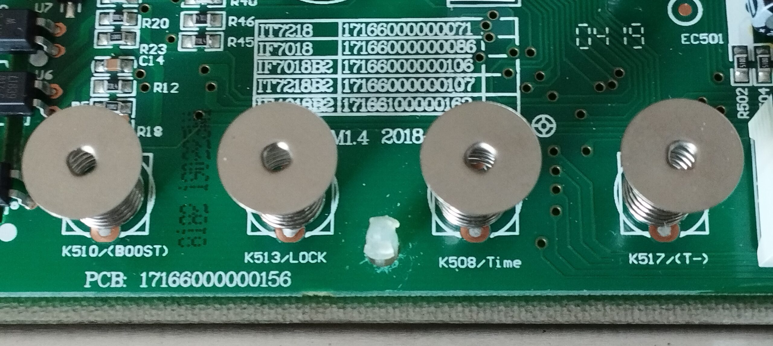
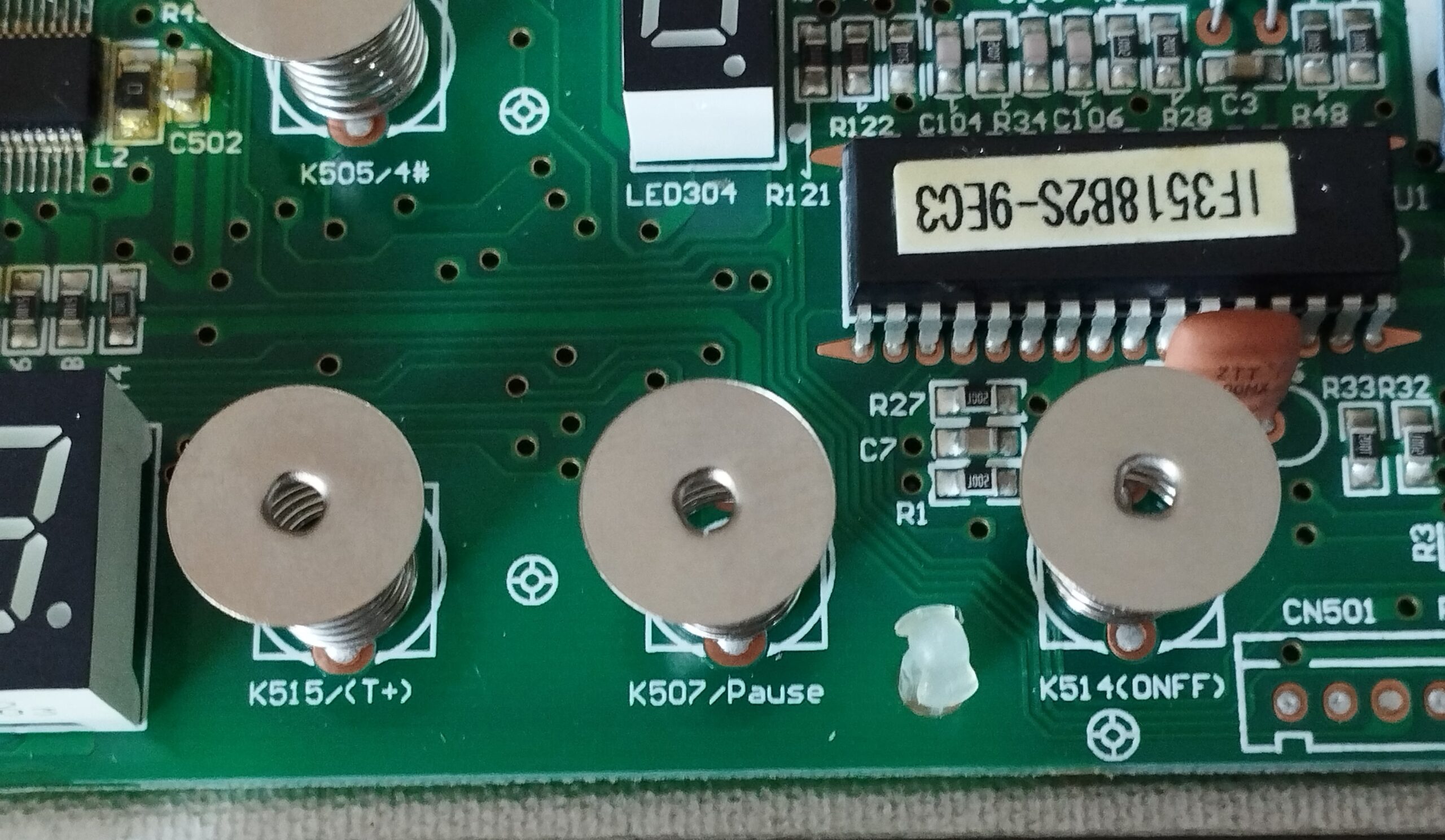
Having a closer look at the interface PCB one thing immediately stands out, there is one extra key on the left side of the keypad! The PCB label of the extra key says “BOOST”, while the boost key on the glass-ceramic surface is the second one from the right labeled with a “P”. The PCB label of that key says “PAUSE” while this stove doesn’t even have this function. The manual confirms that the stove does not have a Pause function, and the “P” key on the glass-ceramic surface is the Boost function.
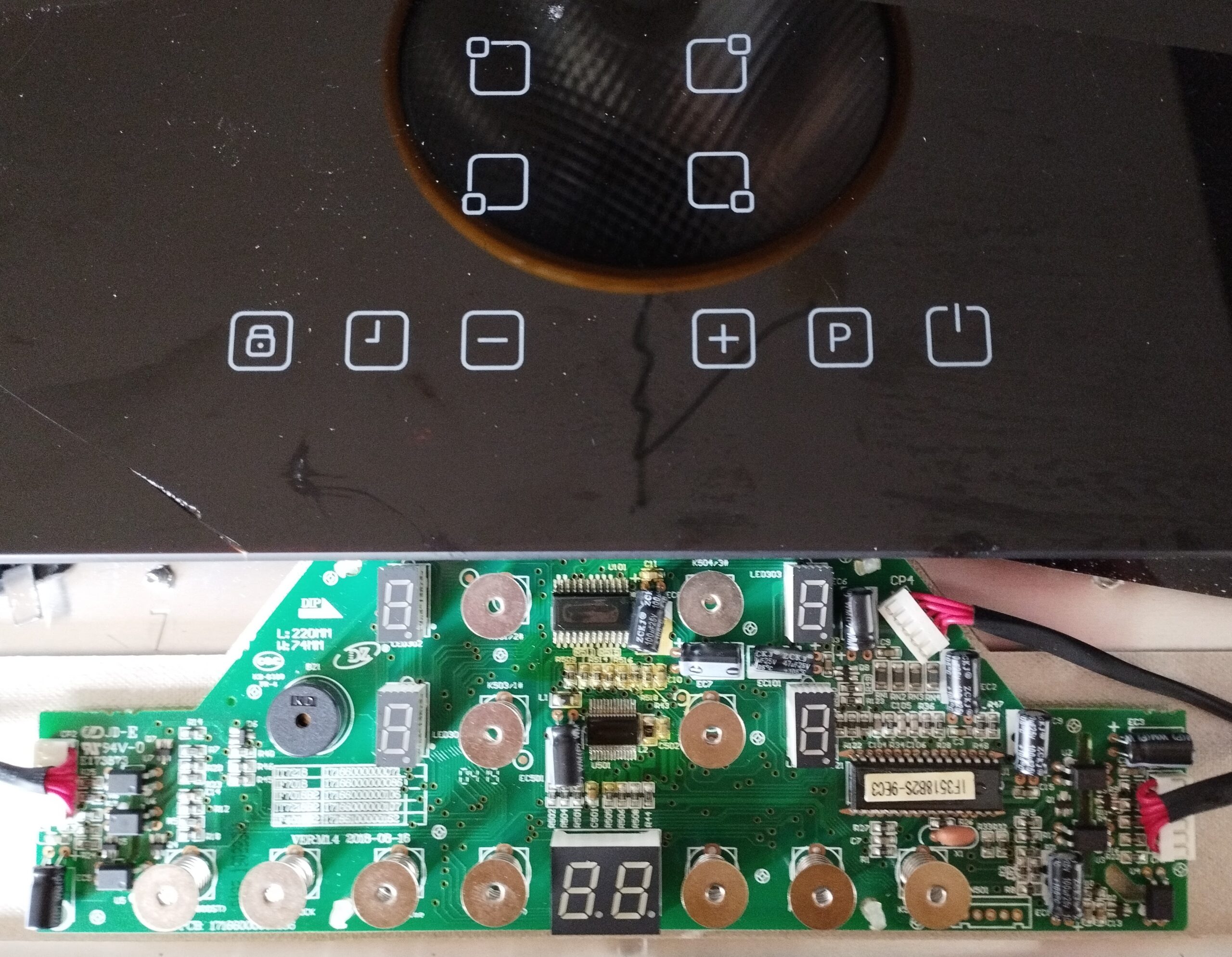
Is this maybe a generic interface PCB used by different models? A quick internet search reveals a very similar board is also used in the Samsung NZ64F3NM1AB and NZ64M3NM1BB.
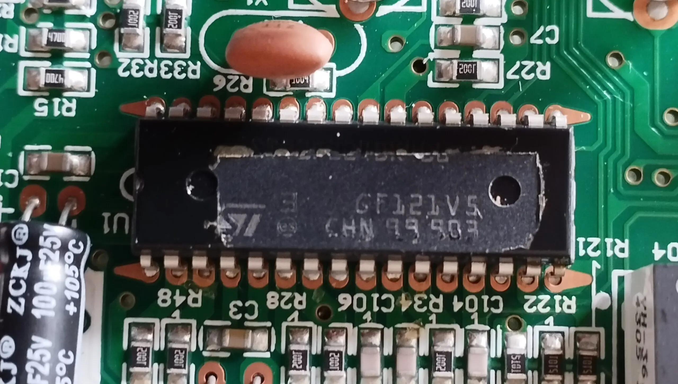
Part of the interface PCB is covered with a conformal coating to protect it against moisture. This makes the labels on the ICs hard to read, but with a bright light under the right angle it’s possible to decipher at least some of the labels.
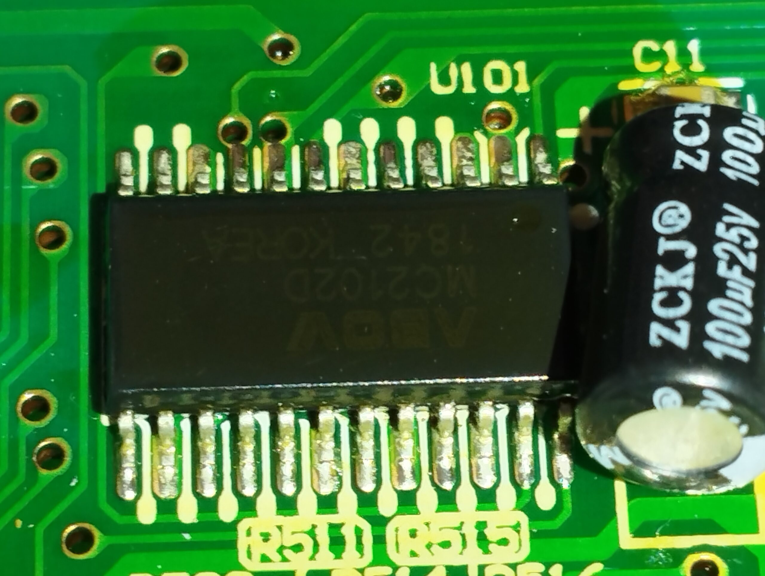
One ICs label reads “ABOV MC2102D 1842 KOREA” which seems to be the driver for the 7 segment LED displays.
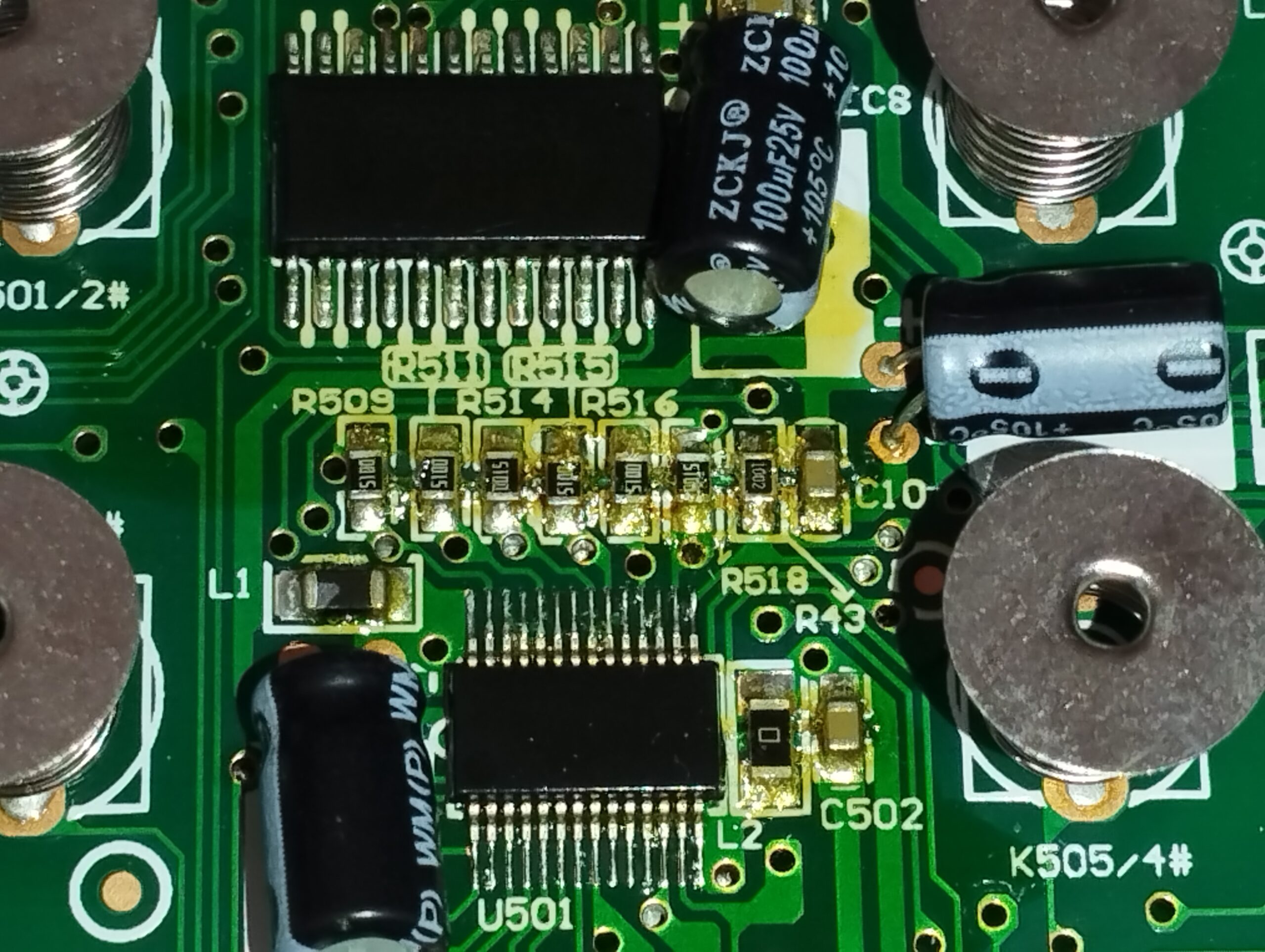
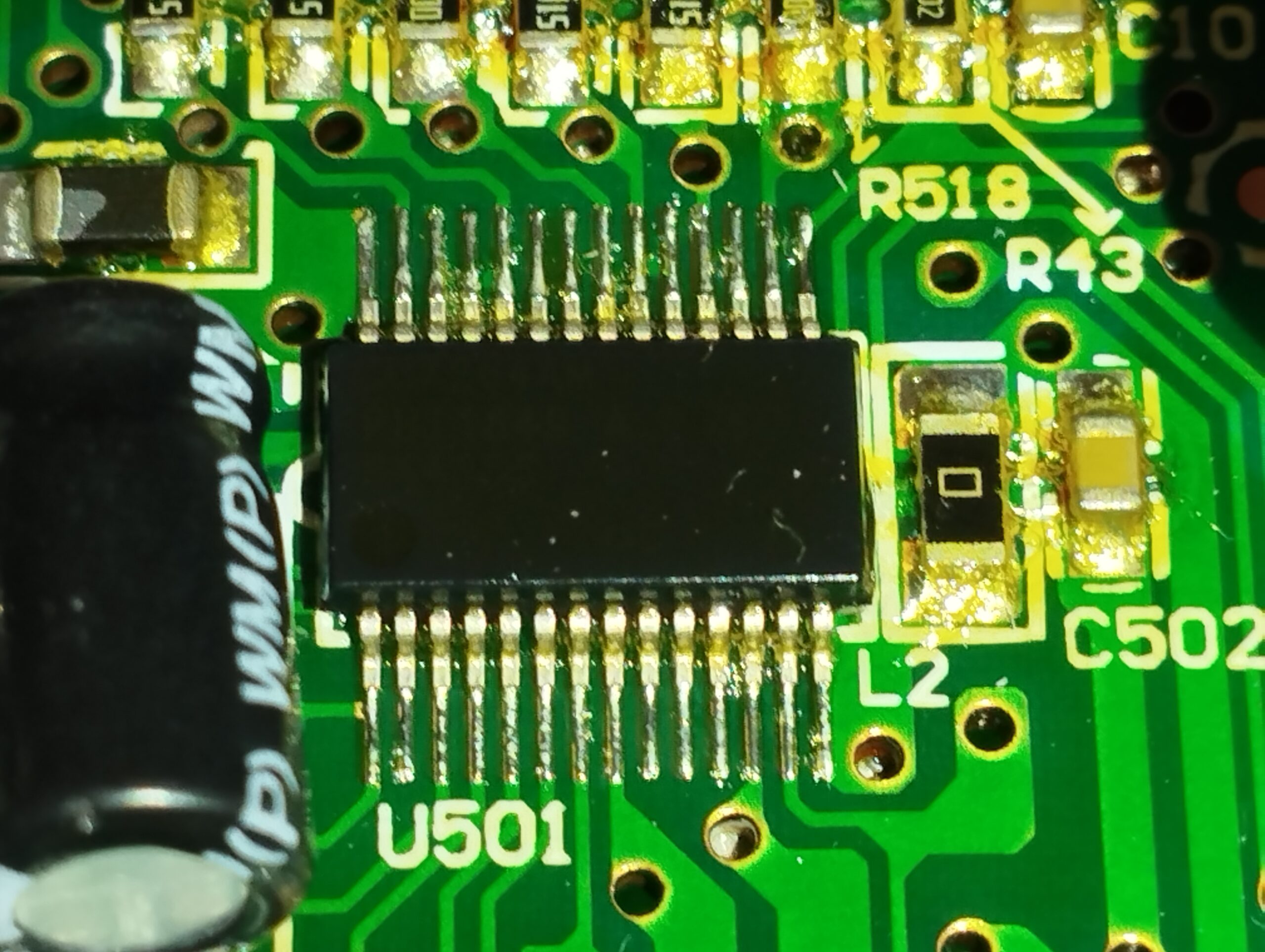
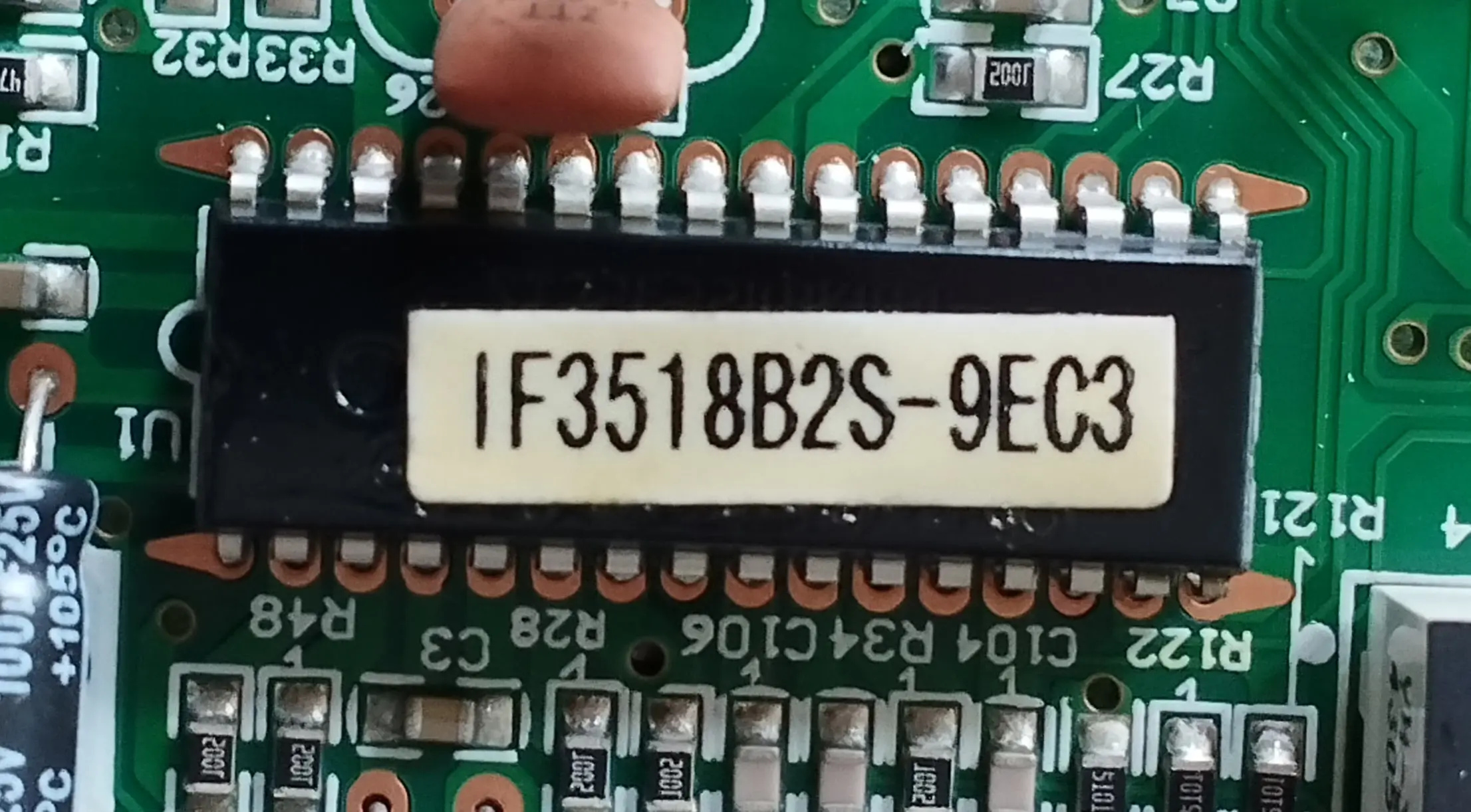
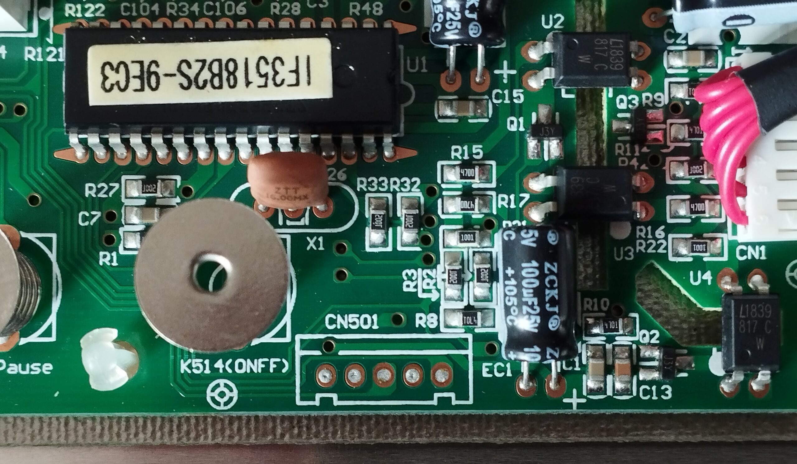
A larger IC on the board has a paper label which reads “IF3518B2S-9EC3” and once removed reveals a label which reads “ST GF121V5 CHN 99903”. There is also some marking on the top part of the IC which is very difficult to read but which is something like “ST7253249K486”.
On the left and right of the interface PCB are two connectors which are isolated from the rest of the circuitry by an air gap and optocouplers.
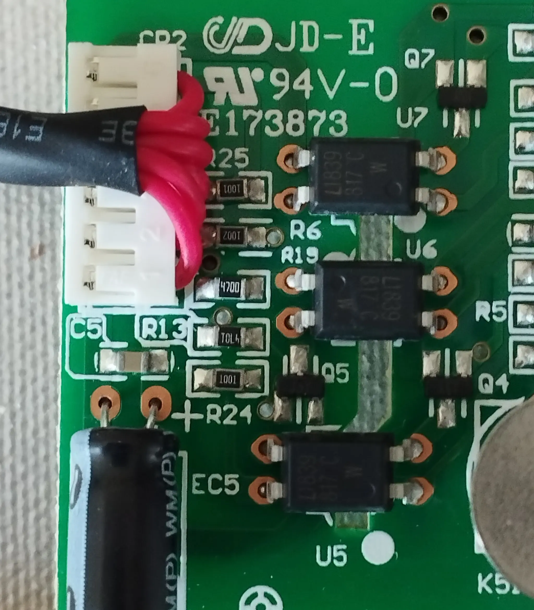
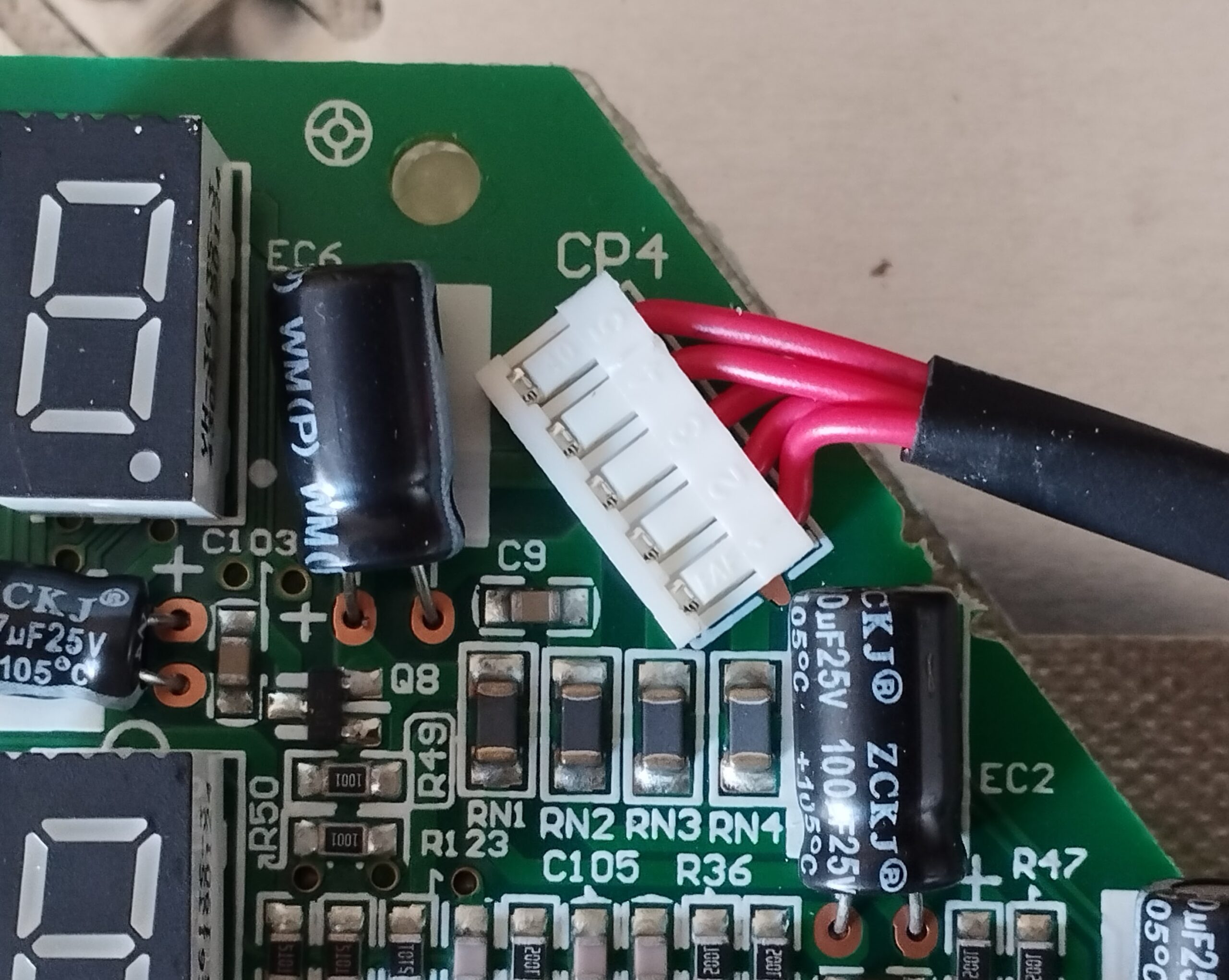
Then there is a connector on the top right of the PCB which is unisolated.
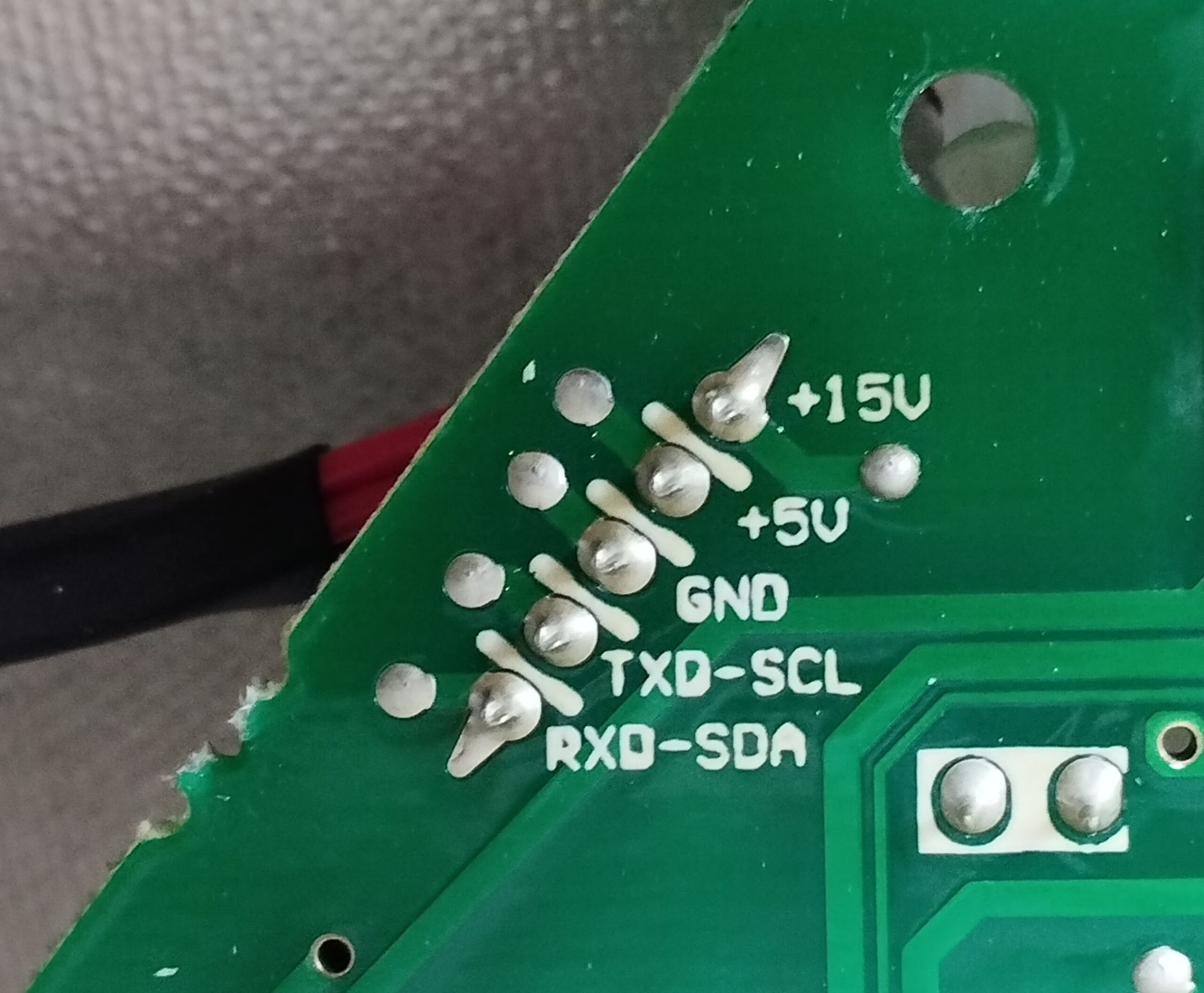
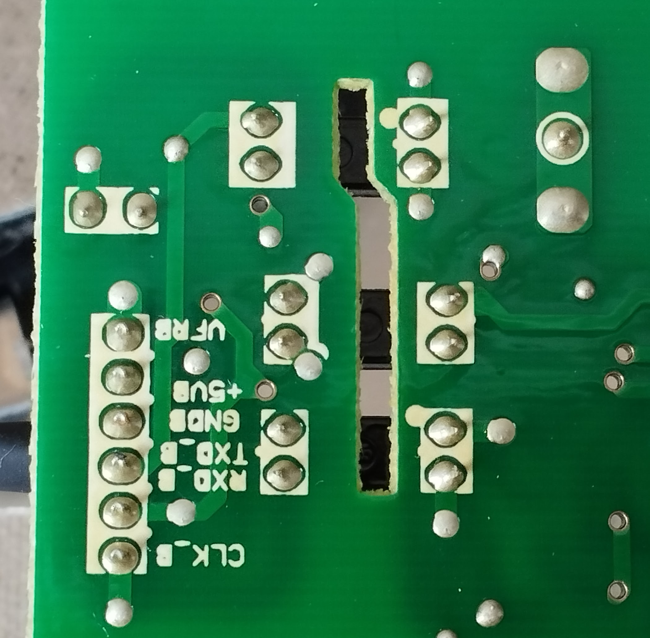
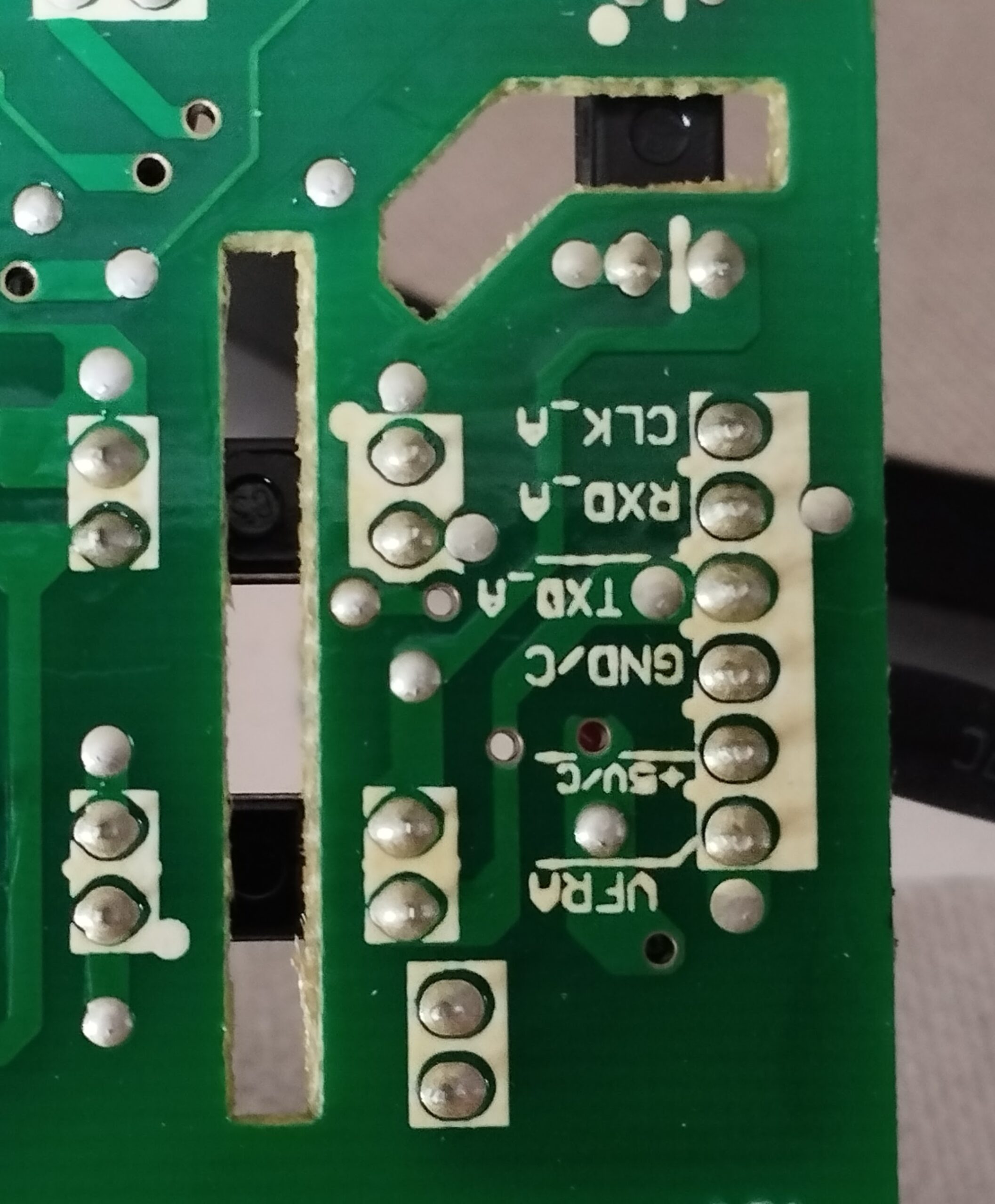
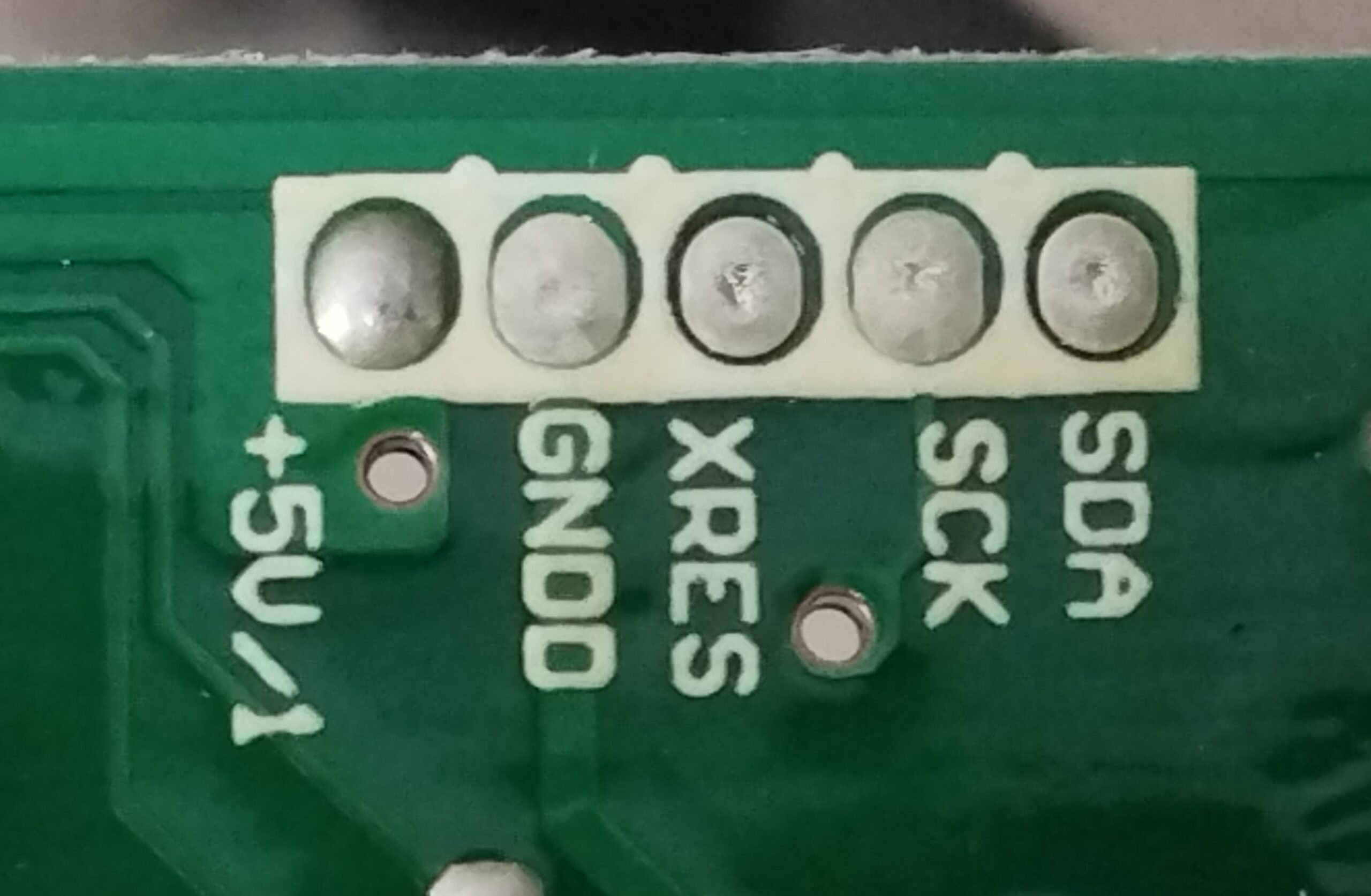
There also is an unpopulated connector on the bottom part of the interface PCB. The labels of the connector reveal the functions of the different pins, and the labels “SCK” and “SDA” give away this is some kind of serial interface. This looks promising!
I think the next thing I can do is connect a probe to the unpopulated connector and do some measurements to figure out which type of serial interface is being used. But that’s something for an other time.
Leave a Reply